ASML: A Monopoly on Magic
The $300 billion Dutch firm is the most important company you’ve never heard of.

Brought to you by Tegus
Have you ever spent hours of time evaluating investment opportunities only to discover that your data isn’t reliable?
Tegus unites insights from credible experts with the best financial data to give you more powerful perspectives for your investment decisions. With top-notch quality across expert calls, transcripts, financial models, and easy-to-cite SEC data, you can gain a unique perspective and ultimately make bold, high-yield investment decisions.
Trial Tegus for free today.
If you only have a few minutes to spare, here’s what investors, operators, and founders should know about ASML.
- An earned monopoly. ASML is the sole provider of EUV lithography machines. These machines use extreme ultraviolet light to create the world’s most powerful semiconductor chips. As one might expect, that’s a valuable position to be in. ASML has a market cap nearing $300 billion and earns tens of billions of dollars annually.
- EUV’s mind-bending complexity. It’s hard to overstate the complexity of ASML’s EUV machines. Each unit has more than 100,000 components sourced from specialty providers, contributing to a $200 million cost. Virtually every step of the machine’s operations involves technological miracles indistinguishable from magic to the layperson.
- Supply chain savants. ASML makes only 15% of an EUV machine’s components in-house. The firm’s genius lies in its ability to coordinate a vast supply chain of manufacturers and integrate their products into a cohesive whole. In some instances, ASML acquires its providers outright, giving it more control over its supply chain.
- The silicon frontier. The Biden administration has aggressively curbed the chip industry’s commercial relationships with China. Since ASML is located in the Netherlands, an American ally, its business is affected by these restrictions, reducing the machines it can send to Chinese customers. The technological conflict between the US and China is a decisive force for businesses like ASML.
- Powering the AI boom. The current artificial intelligence renaissance owes much to ASML. Its machines help create cutting-edge GPUs essential to training and deploying modern AI models. Demand for these chips will likely increase in the coming years, further strengthening ASML’s position. Tomorrow’s most powerful AI experiences will almost certainly rely upon the Dutch firm’s technology.
A parlor game for supervillains: tasked to thwart all human innovation as efficiently as possible, what would you do?
The least creative might suggest a blunt approach – the kind that dominates low-brow thrillers and action flicks. In this banal class, we have the nudged asteroid, conjured epidemic, and detonated caldera. These are weapons that don’t so much end innovation as end, well, everything.
The slightly cleverer fiend might concoct a fresher approach. Why annihilate the world when you could simply snip some subsea internet cables? Why expunge humanity when you could code malware that distorts laboratory measurements and hinders scientific discovery? There are subtler ways to wreak havoc.
These latter suggestions are decent enough, but they’re unlikely to earn much praise from fellow reprobates. If you wish to impress the assorted crowd of calico-stroking-bunker-dwellers, allow me to make a suggestion. The simplest and cleanest way to strangle human progress is to carry a hammer into an ASML laboratory.
The approximately $300 billion Dutch technology firm is the sole manufacturer of extreme ultraviolet (EUV) lithography machines, $200 million contraptions considered by some to be “the most complicated in the world.” These irreplicable marvels of engineering are the result of decades of trial and error, scientific breakthroughs, byzantine supply chains, and billions of dollars. They are irreplicable and, as such, insanely valuable. Without ASML’s EUV technology, it would be impossible to manufacture the world’s most powerful silicon chips – the kinds powering the current artificial intelligence boom. In short, the trajectory of our computational advancement is concentrated in the hands of a provider with a 100% monopoly on a particular kind of magic.
That derailing ASML makes a fitting response to this kind of game is a testament to its unusual, underappreciated power.
How to talk to light
ASML’s EUV lithography is worthy of its title as the world’s most complex machine. With more than 100,000 components, it is a marvel of innovation. It is only thanks to its creation that today’s fabricators can produce chips with transistor gates of just a few nanometers. (If you’re new to the world of chips, you might want to check out our deep dive on TSMC, which covers many of the basics.) The miraculous power of modern phones and computers would not be possible without it. Let’s discuss its magic. We must begin with light.
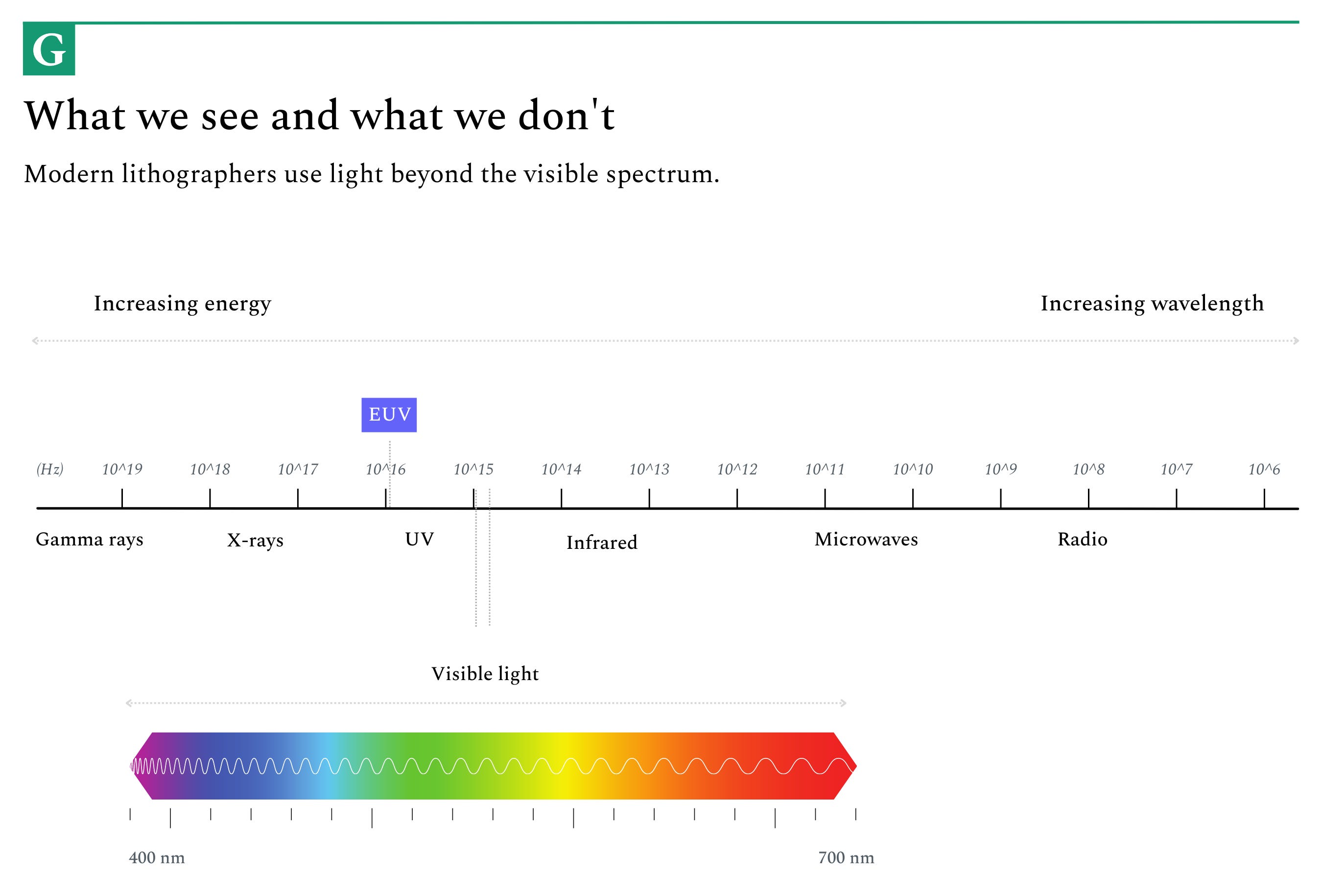
Humans have a strange relationship with the electromagnetic spectrum. We see but a fraction of it – as little as 0.0035%. A tiny sliver accounts for all the color in our lives: the red of a curled rose, green of a tended lawn, ochre of a sunset. To either side are vast territories of invisibility, beyond our perception. There is a hinterland of long, languid wavelengths past visible red composed of infrared, microwaves, and radio. We see the effect of this low-frequency radiation in the billowing steam of a TV dinner and the melody of a favorite song emanating from a car stereo. Travel in the other direction, and you will find another backcountry, a place of short, sharp, high-energy radiation. After violet comes ultraviolet, x-rays, and eventually, gamma rays. Some animals can see these wavelengths – the kestrel that follows a family of voles by the UV-shine of their urine – but we are blind to them.
There are many reasons for ASML’s current dominance. Forced to pick just one, you might say it is a master of the ultraviolet. It understands how to speak to light, how to cajole and persuade, manipulate and bend it.
Recognizing how valuable this is requires a grasp of the importance of semiconductor chips. As covered in our TSMC piece, “semis” are not simply useful but essential – used in computers, phones, vehicles, and weapon systems. According to Chris Miller’s excellent book Chip War, a majority of global GDP is produced by devices that use semiconductors. Because of their ubiquity and utility, they’re also highly strategic, with superpowers like the US and China seeking to control supply and gain an edge.
ASML does not make semiconductors. They make the machine that helps make them. The Dutch company specializes in building “photolithography” or “optical lithography” machines. Effectively, these machines allow you to write with light. With sufficient control and mastery, chip manufacturers like TSMC can use ASML’s creations to turn wavelengths into the tip of a pen and use it to draw transistors onto a silicon surface. These transistors have “gates” acting as switches, turning electric currents into binary data that instructs computing systems. Staying in the realm of magic, we might say photolithography is a kind of incantation: sketch the apposite rune, the felicitous pattern, and watch the metalloids come to life.
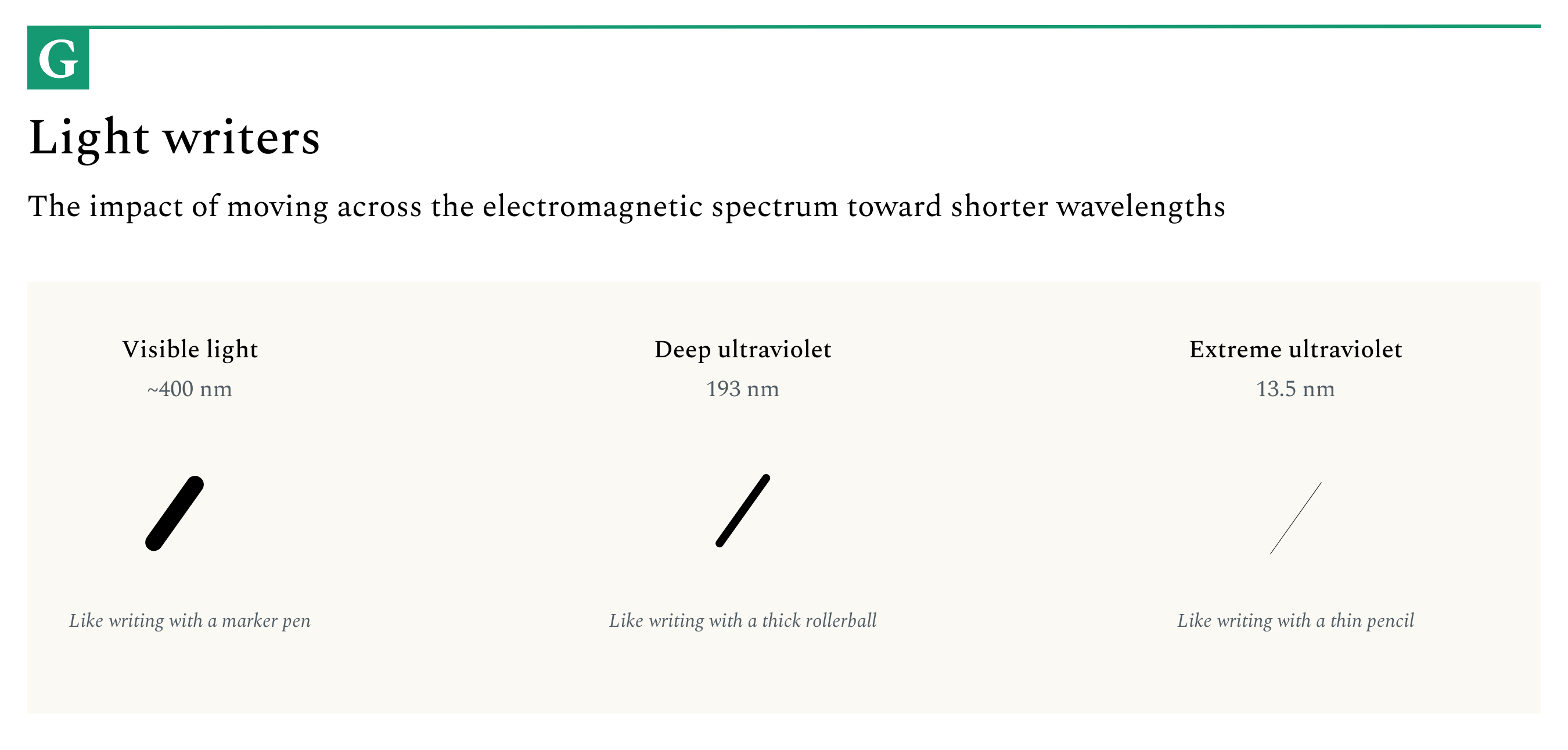
What sets ASML apart from other photolithography providers is the kind of light it uses and how it controls it. Historically, light-writers used the visible spectrum to pattern chips. Wavelengths of 400 to 700 nanometers were sufficient to carve transistors with “gates” north of 1,000 nanometers for most of the 1980s. However, as the industry pushed to cram more and more transistors onto a single chip, increasing their power, photolithographers ran up against a fundamental constraint: visible light was simply too blunt.
To create “sub-micron” transistors – those smaller than 1,000 nanometers – you needed a finer, sharper tool. By the 1990s, companies like Nikon, Canon, and ASML had edged beyond the visible realm into “deep ultraviolet” (DUV) territory, which had a wavelength as low as 193 nanometers. Given the persistence of Moore’s Law, which predicted the number of transistors on a chip would double every two years, these firms understood that soon DUV would be insufficiently dull, too.
So began the rush westward into the outer badlands of the electromagnetic spectrum. At the border of ultraviolet and X-rays is a thin territory of “extreme ultraviolet” light with a wavelength of 13.5 nanometers.
Consider the subtlety and refinement of this instrument. It is approximately 14 times sharper than DUV and 30 times sharper than visible light. If researchers could harness EUV, they could greatly increase the number of transistors per chip. It was the difference between trying to draw delicate lines with a fat marker, a splashy rollerball, or a slim-point pencil.
The quest to wrangle EUV consumed much of the 2000s and 2010s. Though Nikon and Canon invested in commercializing the technology, only ASML managed it. We’ll discuss why ASML succeeded where others failed, but first, we must talk about how.
How did the Dutch company domesticate this wild part of the electromagnetic spectrum? How did it achieve what many researchers and industry observers thought might be impossible?
Let us start with light. You cannot simply buy an EUV bulb and switch it on. Indeed, EUV does not naturally occur on our planet, meaning you have to create it, convince it to emerge. One way to get it is to turn tin into hot plasma. When in this state, the plasma emits EUV light.
This is far from simple. It is difficult to turn tin into plasma, requiring raising its temperature to 500,000 degrees – hotter than the sun. Even in that state, harvesting enough EUV for photolithography is difficult. ASML uses a precision laser developed with a specialty provider, Trumpf, to create the extraordinary heat required.
It took a decade and considerable investment for Trumpf to create a suitable laser at ASML’s behest. Not only must the laser be extremely powerful, it must be fast and accurate, capable of hitting a minuscule ball of tin traveling 200 miles per hour through a vacuum. The laser must, in fact, hit each speck of tin twice to successfully turn it into plasma. To get enough EUV, this process occurs 50,000 times per second. A system of fans turning 1,000 times per second keeps the contraption from overheating as it anoints three million microscopic suns a minute.
Generating EUV is insufficient; you must also figure out how to direct it. This is especially tricky as EUV is highly absorptive – even air absorbs it. That’s why the interior of ASML’s machines operates in a “high vacuum” designed to preserve these emissions.
Though that stops you from losing the EUV created, it doesn’t help you direct it. To solve that problem, ASML once again turned to a partner: Zeiss Group. Founded in 1846 by optician Carl Zeiss, the German firm is an expert manufacturer of “optical systems,” from eyeglasses to microscopes. Buoyed by a $1 billion investment from ASML in 2016, Zeiss produced a flawless mirror composed of 100 layers – each just a few nanometers thick. They are, in Chris Miller’s words, “the smoothest objects ever made.” If scaled up to the size of Zeiss’s native Germany, the mirror’s largest imperfections would still be just a tenth of a millimeter.
ASML’s EUV machines rely on several Zeiss mirrors positioned to direct EUV light to the silicon wafer. Sophisticated software and other critical components ensure the light that reaches the silicon does so in the correct pattern, another complex process. Simply ensuring the disc is in the right place, free of impurities, is challenging. ASML’s machines can position each wafer with quarter nanometer precision, and up to 20,000 microscopic adjustments and checks are conducted per second. If even a single mote of dust lands on the disc, the full batch – which takes months to process – may be ruined.

Given the intricacy of ASML’s EUV machines, it is perhaps unsurprising that operating them requires significant expertise. In some cases, a technical PhD is required, along with intensive operational training. Because using these machines is so difficult, ASML technicians typically accompany them to their destination – a transit that involves 20 trucks, 40 freight containers, and three 747 jets. The technician remains on-site for the duration of the machine’s life, addressing issues and fine-tuning performance.
So important is human capital to ASML’s business, the firm recently announced a commitment to invest “several hundred million euros” to build a research institute in partnership with the Eindhoven University of Technology. The facility will support 500 researchers focused on photolithography, mechatronics, AI, and plasma physics. ASML’s investment will also finance 40 new PhD students per year. It’s an attempt to ensure the company has access to a steady flow of trained talent.
ASML’s playbook
A small joint venture in the Netherlands does not become a $300 billion giant by accident. ASML’s unlikely rise is the consequence of operational excellence, strategic advantages, technological innovation, and a bit of luck. To understand how ASML surpassed the much larger Japanese players like Nikon and Canon, we’ll provide a brief history and explore the firm’s playbook.
ASML’s history is a rich one. Indeed, the tale has so many twists and turns that Dutch journalist René Raaijmakers penned a 600-page-plus book on just the period between the 1960s and mid-1990s. While ASML’s Architects is an ideal chronicle for the chip-obsessed, we can take a briefer approach.
ASML was founded in 1984, the result of a joint venture between electronics firm Philips and Advanced Semiconductor Materials International (ASMI), a maker of chip machines. The partnership aimed to make a foray into the increasingly important photolithography space. Dubbed “ASM Lithography,” workers at the new spin-off were given a leaky shed to work in – located near Philips’ Eindhoven office.
Within a year, ASML released its first machine, building off of research from as far back as the 1970s. In 1986, it debuted another iteration. Despite its productivity, the unit struggled financially, requiring frequent capital injections. These investments became increasingly important as ASML grew its footprint, expanding overseas to the US and establishing ties in Taiwan. Heavy R&D spending was necessary, though it didn’t help matters. By the end of that decade, Philips and ASMI’s generosity had been strained, with the latter stepping away. Only the last-ditch effort of a Philips board member convinced the Dutch parent to continue its support.
It proved a good bet, giving ASML the latitude to launch a new system with significant commercial appeal. The money rolled in, keeping ASML from relying on external capital. By 1995, the firm was on strong enough footing to IPO, listing on the Amsterdam and New York Stock exchanges. ASML had gone from a leaky shed to the public markets in a little more than a decade. Philips would fully divest its stake in the following years, making ASML a truly independent entity.
Although ASML’s IPO was a sign of the firm’s legitimacy, it lagged behind the market leaders. In 1995, Nikon and Canon held 66% market share, compared to the Dutch company’s 18% stake. Few expected ASML to overtake lithography’s big two.
Over the following two-plus decades, ASML would prove the doubters wrong. In the 2000s and 2010s, ASML improved its existing technology and won the EUV race. In truth, it hadn’t been much of a race at all: though Nikon, Canon, and US companies recognized the opportunity, none had the combination of conviction, connections, and capital to pull it off. ASML shipped its first EUV prototype in 2010; by 2020, it had entered high-volume manufacturing.
How did a spin-off on the verge of bankruptcy lap industry power players to build a 100% EUV monopoly? It involved geographical benefits, strategic friendships, and exceptional supply chain management.
A strategic location
Veldhoven is not traditionally seen as an epicenter for technological progress. Located in the southern part of the Netherlands, about 20 kilometers from the Belgian border, it is home to a population of just 45,500. Excluding its connection to ASML, Veldhoven’s claims to fame are links to a handful of politicians and sportspeople and its proximity to Eindhoven’s airport.
While far from possessing the technological vibrancy of Silicon Valley, Beijing, or Tokyo, Verdhoven would nevertheless prove to be a strategic location for the lithography manufacturer. In the battle for chip supremacy between the US and Japan in the 1980s and 1990s, and the US and China today, the Netherlands was a middle ground – albeit one allied with America.
All things being equal, American companies would have preferred giving their lithography business to domestic players. However, during the 1980s, US players like GCA and Perkin-Elmer lost their grip on the market to Nikon and Canon. The result was that American firms had the choice between funding Asian giants that often directly rivaled them or a European upstart. As you might expect, they chose the latter. Micron, a manufacturer of memory chips called “DRAMs,” was particularly important. In 1987, the Boise, Idaho-based firm was the last American holdout in a market that had been all but lost to Japanese players. Rather than give business to Asian rivals, Micron decided to go with ASML.
The research ASML received from US laboratories was even more valuable than the revenue provided by American firms. In the 1990s, Intel invested heavily in EUV research, subsidizing national labs. Insights developed at Lawrence Livermore and National Sandia laboratories were eventually passed to ASML after Intel realized no American firm could effectively commercialize these findings. Nikon and Canon couldn’t get their hands on this information, effectively shutting them out from the EUV revolution. Modern EUV technology rests on discoveries made in America but perfected in Europe.
The right connections
ASML benefited from relationships other than those forged through its connection to American customers and researchers. Most important, of course, was its connection to Philips and ASM International. As noted, these firms provided capital, talent, and research to get the upstart firm off the ground.
Philips’ size and influence provided indirect benefits, too. When Taiwan started a new semiconductor initiative in 1986, the Dutch company agreed to invest $58 million, becoming the first external stakeholder in TSMC. Critically, the Dutch firm agreed to become a customer of the foundry and share its expertise. In his chronicle of ASML, Raaijmakers remarks that Philips held training sessions for TSMC employees, directing its operations so that it could move manufacturing to the upstart foundry. When it came time to purchase lithography machines, ASML was a natural fit, given its Philips DNA and how neatly it synched up with TSMC.
A fire at a TSMC facility in 1988 was a particular boon to ASML. The Dutch firm was struggling for viability at the time, and TSMC’s order for 17 replacement machines helped ASML turn a $7 million profit the following year. Raaijmakers writes, “TSMC’s insurance company – the formal buyer – is ASML’s biggest customer in 1989.” Such moments of serendipity occurred thanks to ASML’s fortuitous connections.
Mastery of the supply chain
Three hundred billion dollar companies do not simply happen. While ASML benefitted from its neutral location, extraneous IP, and strategic connections, its success was of its own making. In particular, the firm mastered the complicated lithography supply chain.
Despite its connection to Philips and ASM International, ASML began life as a resource-constrained organization, especially in the context of the broader semiconductor space. Virtually every step in the chip manufacturing process requires extremely large amounts of capital. Lithography is no different. (As noted, ASML’s most advanced machines fetch $200 million a pop.)
Because of its capital constraints, ASML recognized it could not possibly build a competitive lithography machine from scratch. Each component is impossibly sophisticated, requiring expertise and investment. Instead, it relies on several third-party suppliers, including Zeiss Group, Trumpf, Cymer, and many others. For ASML’s EUV machines, for example, just 15% of components are built in-house; the remaining 85% come from other firms. ASML’s genius is controlling its daedal supply chain and integrating thousands of components.
As alluded to earlier, ASML goes to great lengths to secure its supply chain, investing in key providers as it did by furnishing Zeiss with $1 billion. In cases where it worries about the reliability of a certain provider, ASML will occasionally take the step of acquiring it outright. As documented by Miller, CEO Peter Wennink warned one supplier, “If you don’t behave, we’re going to buy you.” Over the years, ASML has done exactly that. Here are three examples:
- Cymer, $2.5 billion (2012). Cymer is a manufacturer of light sources for lithography. It was early to recognize that pulverizing tin was a promising way to generate EUV. Though ASML would benefit from it, Cymer was first to approach Trumpf to create its precision laser described above. By acquiring Cymer, ASML accelerated its EUV development, helping it land its lucrative monopoly.
- Hermes Microvision, $3.1 billion (2016). After working with Hermes for two years, ASML brought it in-house. The Taiwanese company manufactures “e-beam” inspection equipment that uses electrons to monitor chips and identify microscopic defects. It was a step aimed at boosting production efficiency and supporting EUV.
- Brion Technologies, $270 million (2007). Founded in California, Brion is a computational lithography business. Its tooling helps “optimize and verify” light masks used in lithography. By doing so, it’s able to improve yield.
While ASML is gifted at recognizing when to bring technologies under its umbrella, it is shrewd enough to realize it cannot be entirely vertically integrated. “It’s a matter of time until people realize that the only way to be successful in semiconductors is through cooperation,” an ASML vice president remarked. “The idea that we could go back to a little dark corner and do it all alone is most probably a very challenging concept.”
Three forces
The semiconductor industry is one of constant change, buffeted by commercial, political, and technological winds. While looking too far ahead is a dangerous game, three forces look particularly likely to define ASML’s next decade:
- The AI revolution.
- US-China tensions.
- Maintaining Moore’s Law.
Over the past nine months, Nvidia’s stock has risen more than 300% to reach a $1.15 trillion market cap. It joined an elite quintet in the four-commas-club: Apple, Microsoft, Aramco, Alphabet, and Amazon. Its ascent can be directly attributed to the artificial intelligence boom. Nvidia’s graphic processing units (GPUs) have become essential in training and deploying AI models. Given the paucity of GPU players – and bottlenecks elsewhere in the chip manufacturing process – ratcheting up supply to meet growing demand is not simple. The result is a shortage of some chip models.
ASML stands to benefit from this boom. To manufacture its GPUs, Nvidia relies on TSMC, which relies on ASML. As it looks to push performance further, ASML’s unique EUV abilities will be extremely highly prized. Many of the AI advances we see over the coming years will be indirectly thanks to the Dutch company’s miraculous technology.
ASML’s stock has risen over the same period, but much less than Nvidia’s. In part, that’s because the broader chip industry has entered a slowdown. Different participants in the ecosystem rapidly increased supply during the last bull run to meet growing consumer demand, but as the economy has cooled, purchasing has pulled back. Nevertheless, ASML looks to be in strong shape, recently increasing its guidance for the year after better-than-expected sales in China.
Ultimately, assuming the AI acceleration continues, ASML looks set to become even more powerful. It is the sole provider of an irreplaceable technology.
Though ASML does sell to Chinese companies, it faces heavy restrictions thanks to US sanctions. The cold conflict between Washington and Beijing will inevitably prove critical to ASML’s prospects. As outlined in our TSMC analysis, the Biden administration has moved aggressively to stop China from accessing leading-edge and mid-range chips. In addition to blocking the chips themselves, the sanctions also prevent Chinese customers from receiving the equipment or software necessary to make such chips. Since we published our piece, the government has further curbed exports to China. As a strategic ally, the Dutch government has issued its own controls, reinforcing the restrictions. The harshest of these will come into full effect in September.
From a purely commercial perspective, these limitations are inconvenient for ASML. Its ability to sell EUV or even less advanced DUV machines is manacled, resulting in the loss of billions in revenue. As one would expect, Chinese authorities have a dim view of the current restrictions, with the country’s embassy in the Netherlands chastising its host to “immediately correct its wrongdoings.”
America’s geopolitical agenda also impacts ASML’s hiring. To adhere to US Export Administration Regulations (EAR), the company refuses candidates with certain nationalities or permanent residencies. If a job involves interacting with sensitive US technology, ASML will reject applicants from Iran, Syria, North Korea, Russia, Cuba, and other nations. Failing to do so could result in crippling American sanctions. The Netherlands’ Institute for Human Rights affirmed ASML’s policies after an anti-discrimination group filed a complaint, noting that EAR was “indeed binding for ASML.”
ASML’s prominence owes a great deal to US technology, research, and capital. The price of its ties to the country (and those of its homeland) are significant.
Without ASML’s EUV lithography machine, Moore’s Law might be under threat. “Without this machine, it’s gone,” a researcher told the MIT Technology Review. While ASML’s marvel keeps the industry on track for a little longer, it will inevitably reach a limit. The quest to maintain Moore’s Law drives ASML’s research and development. The company understands the value of a unique technological advantage better than anyone.
So, what comes after EUV? ASML is investing heavily to answer that very question. In 2021, it deployed €2.5 billion to R&D, increasing it to €3.3 billion the following year. In the near-to-medium term, ASML seems to be well poised. Despite their complexity, current EUV machines are considered “basic.” In the next three years, ASML is expected to debut “high numerical aperture” EUV machines that allow for even greater precision. Within a decade, “hyper numerical aperture” versions may come online, though Chip War’s Chris Miller notes their success is far from a foregone conclusion.
As with basic EUV, these machines should usher in a wave of even more powerful chips. As part of its attempt to reestablish itself as the dominant force in chipmaking, Intel plans to invest $95 billion into a “big, honkin’ fab in Europe,” according to CEO Pat Gelsinger. It has struck a deal with ASML to get its hands on high numerical EUV machines first in the hopes of building 2-nanometer chips – a steep reduction from the 7-nanometer nodes that power many smartphones. Several other stakeholders, such as TSMC, are investing in pushing toward 1-nanometer technology. In the not-too-distant future, chips may become so small that we require a new unit of measurement. Already, Gelsinger is proclaiming the advent of the “angstrom era,” an order of magnitude smaller than the nanometer. No firm will be more pivotal to breaching that threshold than ASML. It is the only company capable of turning light into an even finer point.
We do not always keep our technology. History is littered with examples of innovations erased by time. Ancient records tell us that Greek fire was a rare incendiary weapon used by the Byzantines to defend Constantinople in the 7th century. More than a millennium later, we are still unsure exactly what chemicals conspired to create powerful flames that some say sparked when met by water. It is a mystery, a piece of deadly magic lost, forgotten by civilization.
Even the most assured of supervillains would, when pushed, admit a hammer could not derail ASML by itself. (You must allow the devil some poetic license.) But, in the grand scheme of things, it would not take much to extirpate its most vital knowledge from the world. A handful of laboratories leveled to the ground, a couple of hundred EUV machines smashed to rubble, a few thousand choice employees zapped with a memory-erasing pen. And were it to disappear, were its collective expertise to evaporate overnight, it is not unreasonable to think we might not recover it. Chance, skill, genius, and wealth do not always collude so neatly. Like Greek fire, the ability to talk to ultraviolet light would be another extinct marvel that we imagine but cannot know.
The Generalist’s work is provided for informational purposes only and should not be construed as legal, business, investment, or tax advice. You should always do your own research and consult advisors on these subjects. Our work may feature entities in which Generalist Capital, LLC or the author has invested.


Join over 55,000 curious minds.
Join 100,000+ readers and get powerful business analysis delivered straight to your inbox.
No spam. No noise. Unsubscribe any time.